Contactless payment and identification processes are finding their way into more and more areas of our lives. Contactless chip cards are merely a special form of so-called RFID transponders. These are used in a wide variety of forms: as simple door openers, admission wristbands in leisure pools with which you can also pay for food or multifunctional chip cards, which are particularly interesting due to their pocket size.
Structure of a contactless chip card
The main components of a contactless chip card are similar to those of a contact chip card. First of all, you need a chip module, e.g. in the form of a microprocessor circuit, the structure of which is explained in more detail in Part 2.
However, the power supply and data transmission is not via a contact surface, but by using electromagnetic induction. The law of induction states that a current is induced in every electrical conductor that is located in a variable electromagnetic field. This is exploited by building antennas in the form of a coil and having the readers emit alternating magnetic fields or high-frequency radio waves, allowing data and energy to be transmitted. The technical processes for this were adopted from radio and radar technology. The term RFID means Radio-Frequency-Identification, and was first used in the Second World War as a transponder in tanks and aircraft for friend or foe identification. Contactless chip cards are therefore special versions of an RFID transponder.
In order to bring these two main components together in the form of a chip card for the wallet, a carrier material is required. For this purpose, four PVC films of around 0.2 mm thickness are used (the standardized thickness of chip cards is 0.76 mm), two inlet films, which form the core of the card, and two overlay films, which serve as the outer side.
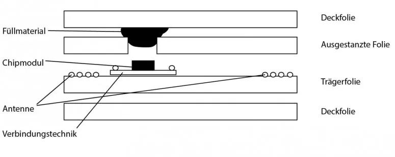
The two cover foils are printed with the layout of the chip cards, which has already been discussed in an earlier blog post.
One of the two inlet foils (carrier foil) is fitted with the antenna coil and this is connected to the chip module. Four different processes were developed to manufacture the coils: winding technology, laying technology, screen printing and etching technology.
The second foil serves as a cover, from which a cavity is punched out to accommodate the chip module of the carrier foil; the remaining cavity is often filled with a potting compound.
Production of the antenna coils
As already mentioned, the coils are produced using different processes:
In the winding technique, the coil is wound on conventional whites, welded to the chip module and then glued to an inlet foil. It is mainly used for low-frequency signals (f<135kHz), as very high numbers of turns are possible.
In the laying technique, the chip modules are first placed on the carrier foil and fixed in place. The coil is then burned directly into the PVC. This is done using a so-called sonotrode, which consists of an ultrasonic transmitter and a wire feedthrough in the head. The ultrasound heats the wire locally to such an extent that it melts into the film. The sonotrode is then moved at the same time and the antenna coil is thus "drawn". The respective ends of the coil are then connected to the chip module using a spot welding system.
Screen printing technology is a widely used process in industry, for example in the production of wallpaper, signs or textiles. In the production of RFID transponders, it is used to print a coil directly onto a film using polymer thick film pastes (PTF = polymer thik film) as the "ink", which consist of powder of a conductive material, a solvent and a synthetic resin for fixing. After drying and evaporation of the solvent, a conductive film remains. It is a very inexpensive process, but only a small number of turns can be produced. 0.1 mm thick RFID inlays, which are mainly used for self-adhesive labels, are used in the high-frequency range, e.g. for smart labels.
Etching technology is a widely used process for the production of printed circuit boards (PCB). In the production of RFID inlays, a wafer-thin (35 µm - 70 µm) copper foil is laminated onto the carrier foil. This is coated with a photoresist, exposed through a positive stencil of the coil to be printed and placed in a developer solution. The photoresist now dissolves in the exposed areas and the copper is removed from all areas that are no longer covered by photoresist in the subsequent etching bath. Finally, only the desired coil remains.
Connection technology and lamination
As the antennas are realized using different processes, different connection techniques are also required between the antenna coil and the chip module.
Coils made of wire are connected using micro-welding technology. To do this, the connecting wire of the coils is insulated at the beginning and end using a special tool and then ultrasonically welded to the contacts of the chip module.
Conventional welding techniques fail with the polymer thick-film pastes of the printed coils. Here, the connection is made using a conductive adhesive or cutting and clamping technology. In the latter case, the chip connections are pierced with a special tool to create two pointed crowns. These are then pressed through the foil onto the respective conductor tracks of the printed coil.
Etched coils are connected using conventional reflow soldering methods, which are used when assembling SMD circuit boards.
In the final step, the individual foils are joined together. This is done by fixing them together precisely and then fusing them in a laminating system under high pressure and by applying heat.
Applications
Public transportation
There is great potential for development here, as printed tickets, which have to be produced in a forgery-proof manner and are usually used up after a single use, are not only unecological, they also cause enormously high costs for transport companies.
Replacing paper tickets with a modern electronic fare management system would benefit everyone involved. Passengers would no longer have to carry cash, and payment processes would be much faster and less complicated. The drivers of small means of transport, who sell the tickets themselves, would be greatly relieved. For the transport companies, the operating and maintenance costs of vending machines would be enormously reduced, billing and the collection of statistical data would be easy and fare evasion would be considerably more difficult.
Around 50 % of all contactless chip cards sold are used for public transport, and large conurbations in Asia in particular rely on electronic ticketing systems. The largest project to date has been realized in the South Korean metropolis of Seoul, where over 8,700 buses were equipped with contactless terminals as early as 1996. In Germany, the Fahrsmart I project was implemented in Lüneburg/Oldenburg as early as 1990, albeit still with contact-based chip cards. In the course of the pilot project, however, considerable shortcomings became apparent. The Fahrsmart II project with contactless chip cards was therefore launched at the beginning of 1995. With this travel system, the passenger has to check in and out for each journey. The collected journey data is transmitted to a central server, where software determines the cheapest ticket (single journey, monthly ticket, etc.) for the routes traveled at the end of each month.
The EU-funded ICARE project has been carrying out field trials with multifunctional chip cards since 1996. In Venice, for example, boat landing stages have been equipped with readers whose tickets can then also be used as admission tickets for museums, hotels or as parking tickets.
Contactless payment transactions
A distinction is made between closed and open payment systems.
Closed systems only work within a specific area for a specific provider. Contactless chip cards have long been used in university canteens and modern soccer stadiums such as the Veltins and Allianz arenas. But other RFID systems, e.g. wristbands in leisure pools, are also used here. In most cases, prepaid systems and simple memory cards are used.
In open systems, the contactless chip cards serve as a cash substitute, they are based on global standards such as the EMV specification (Europay, Mastercard, Visa) and can be used almost worldwide.
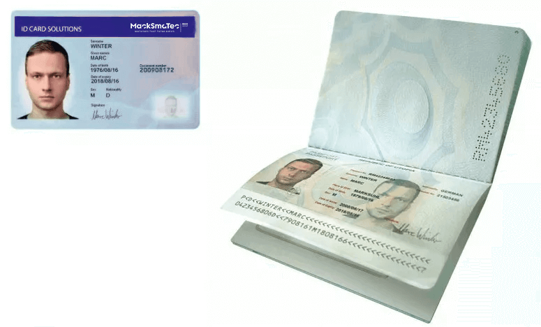
Identity card and electronic passport
The EU passport was introduced in all member states in 2006 in accordance with EU regulations. It is an RFID transponder with a microprocessor in the form of a thin foil that can be integrated into conventional passports. It stores the holder's name, date of birth and gender, as well as a photo of the holder. Since 2008, the holder's fingerprints have also been stored.
The new ID card is a contactless chip card that stores all printed data as well as the photo in higher resolution. If desired, fingerprints can also be stored and electronic proof of identity can be integrated, enabling secure identification in online portals with the help of a reader, for example. It is also possible to retrofit a certificate for digital signatures via private providers.